![]() CAM350 Family 구성
CAM350 Family 구성
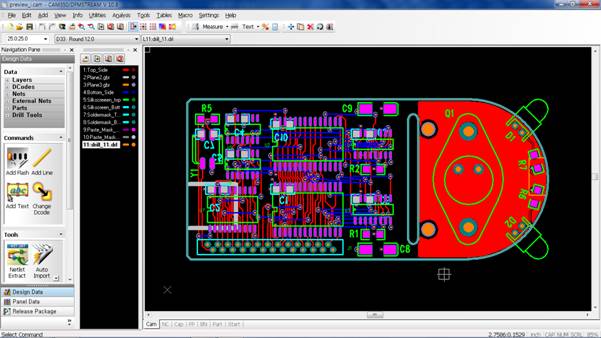
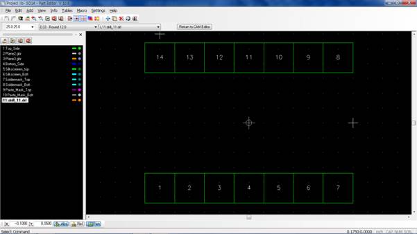
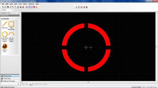
CAM350은 CAM Editor, Part Editor, Cap Editor, Flying Probe Editor, Bed Of Nails Editor, Panel Editor의 프로그램으로 구성되어 있습니다.
- CAM Editor : 일반적인 CAM작업 할 수 있는 프로그램
- Part Editor : 부품을 만들거나 수정 가능한 프로그램
- Cap Editor : 사용자 정의 Aperture를 제작할 수 있는 프로그램
- Flying Probe Editor와 Bed Of Nails Editor : BBT용 드릴 데이터를 생성하는 프로그램
- Panel Editor : 판넬 작업만을 자동으로 처리해주는 내부프로그램
각각의 프로그램은 별도로 존재하는 것이 아니며 CAM350내 Tool 메뉴에서 선택하면 각각의 프로그램으로 바뀌어 집니다. 초기에 CAM350을 실행하면 나타나는 화면은 CAM Editor이며, CAM Editor와 Cap Editor를 제외한 나머지는 모두 Option입니다.
< CAM Editor > < Panel Editor >
< Bed of Nails Editor > < Flying Probe Editor >
< Part Editor > < Cap Editor >
<< 특 징 >>
CAM350은 CAM 시장에서 가장 강력하고, 포괄적인 해법을 제공하는 툴이라고 할 수 있으며, PCB 제조회사나 디자이너들에게 쉽고 간편하게 데이터를 확인 수정할 수 있도록 만들어져있습니다. 다양한 포맷의 데이터 입출력은 물론 최적화 된 드릴 및 라우터 데이터 , BBT용 데이터 작성, 효과적인 Panelization 작업, 이 모든 과정이 자동화된 프로세서를 통해 이루어지게 됩니다. 또한 DFF Analysis를 통해 제조과정에서 발생 가능한 문제점을 사전에 파악하여 시간과 비용을 절감할 수 있습니다.
CAM350 시리즈는 Windows 7, 8 (32bit, 64bit)등에 설치가 가능하며,수년간의 기술 개발로 현재 가장 강력하고 쓰기 쉬운 툴이 되었습니다. 현재 최종버전인 11.x 버전의 경우 디자인 확인을 주로 하는 PCB 디자이너와 PCB 제조분야 CAM 엔지니어 모두의 요구에 맞게 모듈별로 개발이 되어 있어 원하는 옵션만을 선택적으로 구입 하실 수 가 있습니다.
![]() 데이터 입/출력
데이터 입/출력
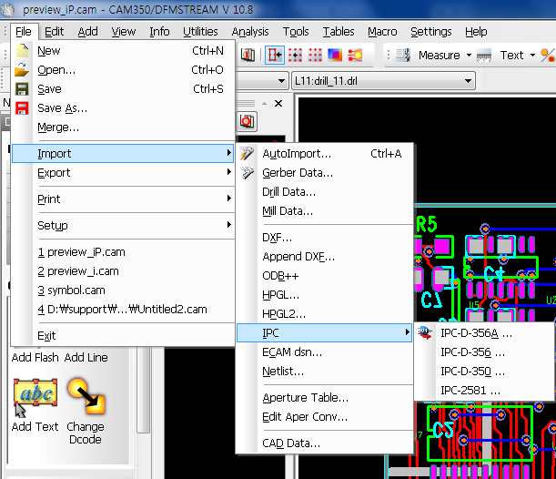
CAM350은 ODB++, Gerber, DirectCAM, IPC D-356 등의 다양한 포맷의 데이터와 호환이 아주 뛰어난 제품입니다. 또한 옵션에 따라서 PowerPCB 등의 CAD 데이터베이스를 바로 입력이 가능합니다.
![]() 데이터 입/출력 시 사용가능한 기능
데이터 입/출력 시 사용가능한 기능
- Reverse Engineering
- Draw-to-Raster Polygon Conversion
- Composite-to-Layer
![]() 자동화 툴과 스크립트
자동화 툴과 스크립트
CAM350에서는 작업의 정확성, 효율성을 위해 배치모드에 의한 자동화를 가능하게 해 줍니다.
Quote Agent 와 MRC Agent라는 사용자 설정이 가능한 두가지 자동화 툴을 통해 좀더 쉽게 데이터에 대한 분석 결과를 얻을 수 있습니다.
Quote Agent는 견적에 필요한 모든 자료들을 찾아서 리스트 해주며 MRC Agent는 80가지의 서로다른 검사를 한번에 처리하여 데이터의 이상유무, 난이도 등의 결과를 분석해 줍니다.사를 한번에 처리하여 데이터의 이상유무, 난이도 등의 결과를 분석해 줍니다.
![]() 제조를 고려한 디자인
제조를 고려한 디자인
DFF 분석 기능을 통해 80가지 필수 검사를 실시하여 제조 Spec에 벗어나는 오류를 사전에 방지해 줍니다.
(Silk Screen, Power and Ground layer, Signal layer, Drill, Solder mask)
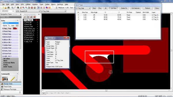
사전에 불량 포인터의 검색, 확인 및 자동 수정등이 가능하며 Acid trap, Soldermask sliver, Copper sliver, Starved thermal 등의 검사를 시행할 수 있습니다.
![]() 뛰어난 Data 변환
뛰어난 Data 변환
Draw-to-Flash, Vector-to-Raster, Polygon conversion, Silkscreen clipping 과 내층 레이어 무기능 패드 삭제등 다양한 데이터 변환 툴이 있습니다.
![]() CAD 데이터 입/출력
CAD 데이터 입/출력
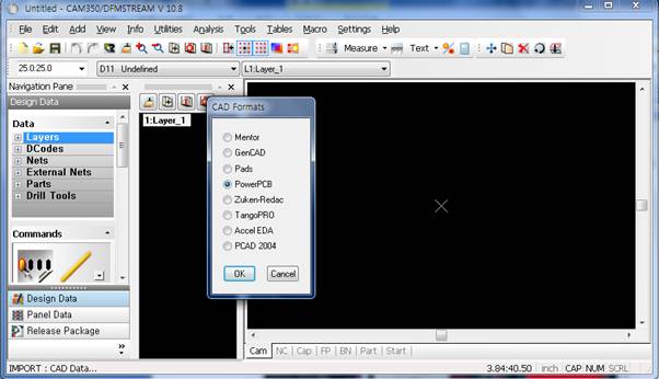
CAM350의 DirectCAD 기능을 사용하여 CAD 데이터베이스를 직접 입/출력할 수 있습니다. 이때 자동으로 데이터의 속성을 함께 가져올 수 있으며, Gerber 파일로 작업해야하는 수고를 덜 수 있습니다.이렇게 함으로써 Drawn 데이터를 줄일 수 있을뿐만 아니라 좀더 완전한 네트리스트를 생성할 수 있습니다.
테스터포인터, 홀, 네트리스트와 부품 풋프린트등의 모든 정보들을 CAM350으로 가져와 저장할 수 있습니다.
![]() Autocad의 DXF 데이터 입/출력
Autocad의 DXF 데이터 입/출력
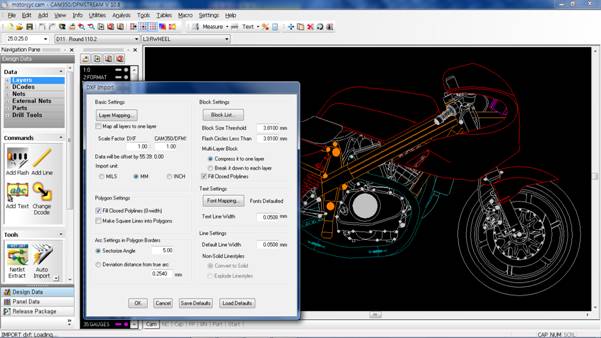
반도체 디자인과 같은 정밀함이 요구되는 Artwork의 경우 Autocad에서 작업이 이루어 지는 경우가 많은데, 실제 PCB를 제조하기 위해서는 Gerber 포맷으로의 전환이 필수입니다. CAM350에서는 Autocad의 Text, font, Raster – Fill 처리된 폴리건, Taper 처리된 라인 또는 아크, 라인 스타일 등을 그대로 유지한채로 입/출력 처리를 할 수 있습니다.
![]() 디자인 룰 검사
디자인 룰 검사
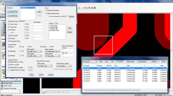
CAM350에는 MRC (Manufacture Rules Check)기능이 있어 Track-to-Track, Track-to-Pad, Pad-to-Pad 등과 같은 다양한 타입의 공간 에러 뿐만 아니라 패드가 없는 드릴, 드릴이 없는 패드 등에 대한 검사를 할 수 있습니다. 게다가 MRC는 Drill-to-Mask, Mask-to-Pad, Drill-to-Pad에 대한 Annular ring 문제 또한 검사 할 수 있습니다. 여러개 항목에 대해서 설정 및 Batch 모드에 의한 검사 또한 가능 합니다.
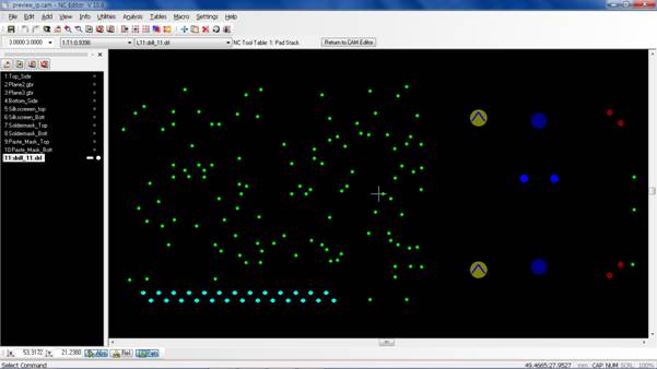
![]() NC 데이터의 편집
NC 데이터의 편집
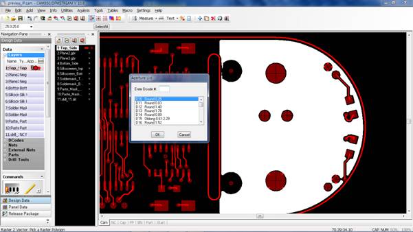
CAM350에는 NC Editor 라는 내부 툴이 별도 있기 때문에 내부에서 모든 작업을 처리할 수 있습니다. 이 Editor를 통해 일반 CAM editor 에서와 같이 쉽게 드릴 (라우터) 편집을 할 수 있게되며, 다양한 기능을 사용하여 데이터의 최적화를 할 수 있게 됩니다.
![]() Symbol Editor
Symbol Editor
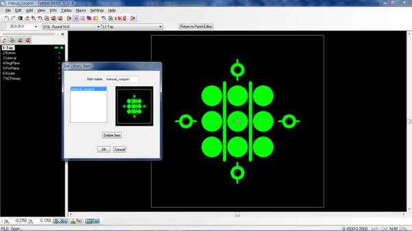
심볼은 판넬 작업 시 사용되는 각종 식자를 말하며 자주 사용되는 심볼들을 특정 라이브러리에 저장해 두었다 필요에 따라 사용하게 됩니다. 본 Editor에서는 이 심볼들을 원하는 모양으로 편집 할 수 있게 해줍니다.
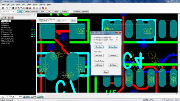
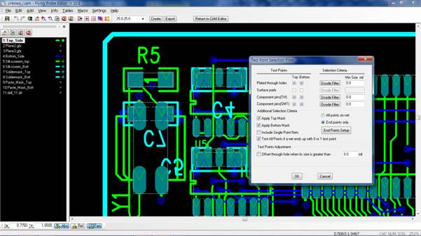
![]() Bare Board Test
Bare Board Test
CAM350 에는 Flying Probe 와 Bed-of-Nails 테스터 장비를 구동하는데 필요한 데이터를 출력할 수 있는 bare-baord test editor가 있습니다. 이 기능을 통해 검사 장비의 능력을 최적화하고 정확한 네트리스트를 생성하며 충돌, 깨짐, 프로브 되지 않는 포인터등을 검색해주게 됩니다.
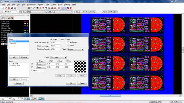
![]() Panel Editor
Panel Editor
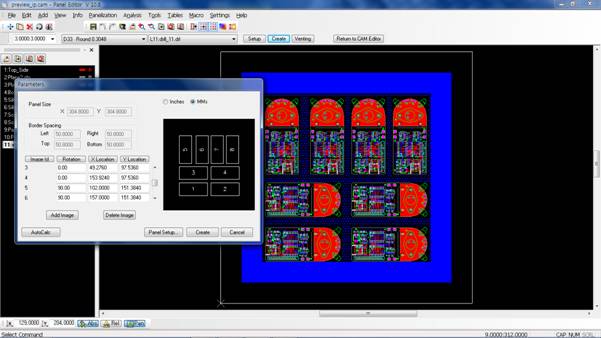
CAM350에서 판넬 에디터는 작업자가 다양한 판넬 크기 별로 다양한 탬플릿을 미리 제작해 두었다가 판넬 작업시 사용함으로써 보다 정확하고 빠른 작업을 가능하게 해줍니다. 각 탬플릿에는 Pinning hole, 테스트 쿠폰, 타이틀 블록과 인식마크등이 추가될 수 있으며 Step &Repeat 간격과 판넬 외곽간 간격등이 설정되어 수작업에 의한 오류를 최소화 할 수 있습니다.
판넬 에디터에서는 또한 “Spreadsheet” 모드를 통해 최대 수율을 얻기 위해 PCB의 방향을 서로 다른 방향으로 회전할 수 있습니다.
![]() 스크립트
스크립트
견적을 내거나 룰 체크를 하는데 사용되는 ,Procss Agent라고 불리는 몇가지 스크립트들이 기본 또는 옵션으로 내장되어 있어 작업을 좀더 용이하게 해줍니다.
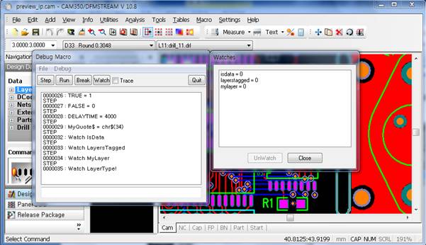
숙련된 프로그래머일 경우 BASIC 프로그래밍 언어를 사용하여 CAM350의 매크로 스크립트 기능을 사용할 경우 복잡한 작업과정들을 자동화 함으로써 생산성면에서 높은 이득을 가질 수 있습니다.
![]() Basic Streams DFM(DFMStream 200)과 Advanced Streams DFM(DFMStream 500)
Basic Streams DFM(DFMStream 200)과 Advanced Streams DFM(DFMStream 500)
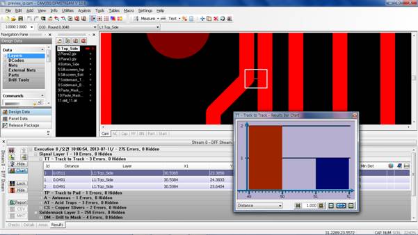
CAM350에서 DRC 및 DFF analysis의 설정, 수행, 분석을 한번에 수행할 수 있습니다. 기존에는 설계 데이터와 고객의 요구에 따라 검사의 종류와 방법이 달라집니다. 그리고 하나의 PCB 작업을 할 때마다, 각각의 검사 항목을 일일이 새로 설정한 후, 각각의 항목을 일일이 실행시켜야 하는 불편함이 있었습니다. 하지만 9.x 버전부터 지원하는 Stream RC 기능을 이용하여 여러 검사 항목과 설정을 하나의 그룹으로 만들어 저장할 수 있습니다. 따라서 생산 시 필요한 그룹을 불러들여 한 번에 여러 검사를 실행하고, 검사에서 발견된 오류를 보기 쉽게 표시해 줍니다.
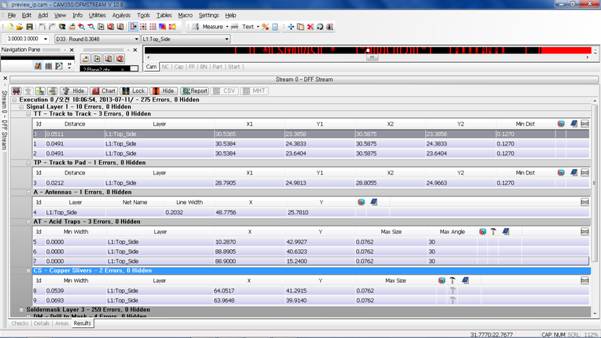
[ Basic Streams DFM(DFM Stream200)과 Advanced Streams DFM(DFMStream 500)의 검사 항목 ]
Preprocess
Draw to Raster Polygon Conversion, Remove Covered Data, Auto Detect and Exclude Text Areas, Remove Pads Smaller than Drills, Remove Redundant Pads, Copy Shadow Database over Original Database
Signal Layer
1) Basic Streams DFM
: Track to Track, Track to Pad, Pad to Pad, Pad to Drill, Minimum Track, Minimum Pad, Unplated Drills to Copper, Plated Drills to Copper, Copper to One-up-border, Redundant Pads, Plated Drills without Pads, Pads without Drills, Antennas, Minimum Gap, Minimum Width, Acid Traps, Copper Slivers, Pin Holes
2) Advanced Streams DFM
: Copper Spacing – Track to Track, Track to Copper, Copper to Copper, Track to Pad, Copper to Pad
Pad Spacing – Flash to Flash, Component Pin to Component Pin, SMD to SMD, Via to Via,
Laser Via to Laser Via, Through pad to Through pad, SMD to Via, SMD to Laser Via,
SMD to Through pad, Via to Through pad, Laser Via to Through pad
Drill Spacing – Unplated Through Hole Drill to Pad, Unplaed Through Hole Drill to Track,
Back Drill to Copper, Back Drill to Pad, Back Drill to Track, Through Hole Drill to
Copper, Through Hole Drill to Pad, Through Hole Drill to Track, Via Drill to Copper,
Via Drill to Pad, Via Drill to Track, Laser Via Drill to Copper, Laser Via Drill to Pad,
Laser Via Drill to track
Annular Ring– Component Pin Pad to Drill, Pressfit Pin Pad, Via to Drill, Laser Via to Drill,
Blind Via to Drill, Buried Via to Drill, Pad to Unplated Drill
Positive Plane
1) Basic Streams DFM
: Plated Drills to Copper, Unplated drills to Copper, Pads to Drills, Acid Traps, Copper Slivers, Pin Holes, Minimum Gap, Minimum width
2) Advanced Streams DFM
: Board Outline Spacing Checks – Copper to One Up Border, Copper to Rout, Copper to Mill Tab
Drill spacing checks – Unplated Through Hole Drill to Copper, Unplated Through Hole Drill to Pad, Unplated Through Hole Drill to Track, Back Drill to Copper, Back Drill to Pad, Back Drill to Track, Through Hole Drill to Copper, Through Hole Drill to Pad, Through Hole Drill to Track, Via Drill to Copper, Via Drill to Pad, Via Drill to Track, Laser Via Drill to Copper, Laser Via Drill to Pad, Laser Via Drill to Track
Annular Ring Checks – include Component Pin Pad to Drill, Pressfit Pin Pad, Via to Drill, Laser Via to Drill, Blind Via to Drill, Buried Via to Drill, Pad to Unplated Drill.
Others – Minimum Gap, Minimum Width, Acid Traps, Copper Slivers, Pin Holes
Negative Plane
1) Basic Streams DFM
: Plated Drills to Copper, Unplated Drills to Copper, Pads to Drills, Copper to One-Up-Border, Isolated Thermal, Starved Thermal, Thermal Conflict, Tie Width
2) Advanced Streams DFM
: Board Outline spacing checks – Copper to One Up Border, Copper to Rout, and Copper to Mill Tab
Drill spacing checks – Through Hole Drill to Copper, Via Drill to Copper, Laser Via Drill to Copper, Unplated Through Hole Drill to Copper, Back Drill to Copper
Annular Ring checks – Pad to Drill, Via to Drill, Laser Via to Drill, Blind Via to Drill, Buried Via to Drill
Others – Isolated Thermal, Starved Thermal, Thermal Conflict, Tie Width
Soldermask
1) Basic Streams DFM
: Pad to Mask, Drill to Mask, Mask Slivers, Solder Mask Bridge, Pin Holes, Solder Mask to Track, Missing Solder Mask
2) Advanced Streams DFM
: Pad Annular Ring checks – SMD to Mask, Plated Drill Pad to Mask, Unplated Drill Pad to Mask, Undrilled Pad to Mask, Via Pad to Mask, Laser Via Pad to Mask.
Drill Annular Ring checks – Plated Through Drill to Mask, Unplated Through Drill to Mask, Via Drill to Mask, Laser Via Drill to Mask.
Silkscreen
1) Basic Streams DFM
: Silkscreen to Soldermask, Minimum Soldermask Width
2) Advanced Streams DFM
: Silkscreen to Solder Mask, Minimum Solder Mask Width, Silkscreen to Board Outline
NC Data Layer
1) Basic Streams DFM
: Overlapping Hits, Coincidental Hits, Redundant Hits, Drill to Drill, Imploded Arcs, Imploded Path, Mill Tab Errors
2) Advanced Streams DFM
: Overlapping Hits, Coincidental Hits, Redundant Hits, Drill to Drill, Imploded Arcs, Imploded Path, Mill Tab Errors, Aspect Ratio
Pastemask
1) Basic Streams DFM
: Paste Mask on Through Holes, Missing Paste Mask on SMD Pads, Missing Solder Mask for Paste Mask Pads, Paste Mask to Copper clearance
2) Advanced Streams DFM
: Paste Mask on Through Holes, Missing Paste Mask on SMD Pads, Missing Solder Mask for Paste Mask Pads, Paste Mask to Copper clearance, Global Fiducials Checks, Paste Mask Pad Aspect Ratio, Paste Mask Pad Area Ratio, Paste Minimum Width
Netlist Compare
Import External Netlist, Extract CAM Netlist, Run Netlist Compare
Design Compare
Import CAM350 file (*.CAM), Run Design Compare
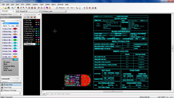
Design Analyzer
Design Analysis reporting, including User Parameter specifications, Calculated desgin analysis and customized output formatting